Pin Mapping
Every DUELink module utilizes a unified pin mapping system, sharing identical features and hardware limitations. To simplify development, the GPIO numbering is abstracted, meaning the pin numbers you use in code do not correspond one-to-one with the physical pins on the underlying microcontroller.
Standard Lib Pins
The DUELink system features automatic pin configuration. It intelligently detects which standard library function is being called and automatically handles the necessary mapping and configuration for that specific pin behind the scenes.
For example, Dwrite(1, level) will automatically change pin 1 to output and write it to level. Similarly, AWrite(1, 0.33) will change pin 1 to its analog feature (PWM) and then set the duty-cycle to 33%.
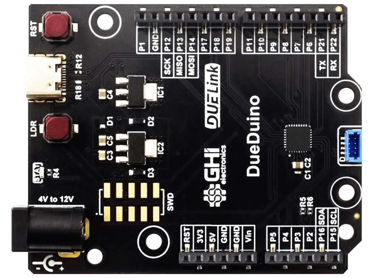
While all modules' schematics are provided, extra efforts are made so you do not need to look up any schematics. When using a module that exposes the pins directly, the pin numbers are listed right on the PCB, just like we have them on DueDuino.
Modules ship with Driver Script. This eliminates the need for accessing pins directly. Samples on using the driver is found on individual modules product pages.
Alternate Functions
All pins support digital input and output. However, some pins have alternate functions.
Pin P0 is always connected to STAT LED. In some rare cases the STAT LED becomes part of an LED matrix.
Pins equipped with alternate functions:
- Analog: P1, P2, P3, P4, P5, P6, P7, P8, P9, P17.
- PWM: P0, P1, P2, P3, P4, P5, P6, P7, P8, P11.
- Interrupt: P1, P2, P3, P4, P5, P6, P7, P12, P20.
System Timers
System timers are used by some of the standard library functions plus for generating PWM signals, for example when using AWritre(), Servo(), or Freq().
Timers can control more than one pin. They are listed here with their used pins:
| Timer | Pins |
|---|---|
| TIM1 | P1, P2 |
| TIM2 | P4, P11 |
| TIM3 | P5, P6, P7, P8 |
| TIM14 | P3 |
| TIM16 | P0 (STAT) |
Pins that share the same timer will share the same frequency, but will always have an independent duty-cycle. For example, changing the frequency on P2 will also change the frequency on P1. This is not an issue of both pins are used to dim LEDs, but will be an issue of P1 is used to dim an LED but P2 is connected to a buzzer.
When designing a module, we use different timers for different functionalities.
Map Table
This table shows how the official firmware maps the pins internally. This is all automated by the system and should not be used by you, unless you are building a special firmware!
| DUELink Pin | ST Micro Pin | Analog | PWM | Interrupt | Alternate Function |
|---|---|---|---|---|---|
| 0 | PB8 | STAT LED | |||
| 1 | PA0 | ADC0 | T1C1 | ✓ | |
| 2 | PA1 | ADC1 | T1C2 | ✓ | |
| 3 | PA4 | ADC4 | T14C1 | ✓ | |
| 4 | PA5 | ADC5 | T2C1 | ✓ | |
| 5 | PA6 | ADC6 | T3C1 | ✓ | |
| 6 | PA7 | ADC7 | T3C2 | ✓ | |
| 7 | PA8 | ADC8 | T3C3 | ✓ | |
| 8 | PB1 | ADC18 | T3C4 | ||
| 9 | PB0 | ADC17 | |||
| 10 | PC15 | ||||
| 11 | PC6 | T2C3 | |||
| 12 | PB3 | ✓ | SPI CLK | ||
| 13 | PB4 | SPI MISO | |||
| 14 | PB5 | SPI MOSI | |||
| 15 | PB6 | I2C SCL | |||
| 16 | PB7 | I2C SDA | |||
| 17 | PB2 | ADC19 | |||
| 18 | PB9 | ||||
| 19 | PA15 | ||||
| 20 | PA14 | ✓ | LDR / SWDCLK | ||
| 21 | PA9 | Uplink (UART TX)﹡ | |||
| 22 | PA10 | Uplink (UART RX)﹡ | |||
| 23 | PA13 | ADC13 | SWDIO | ||
| 24 | PC14 | ||||
| 25 | PA2 | Downlink TX | |||
| 26 | PA3 | Downlink RX | |||
| 27 | PF2 | Reset |
﹡These pins are only available for UART when the module has a USB connector and does not need a Uplink JST connector.